|


50Ω
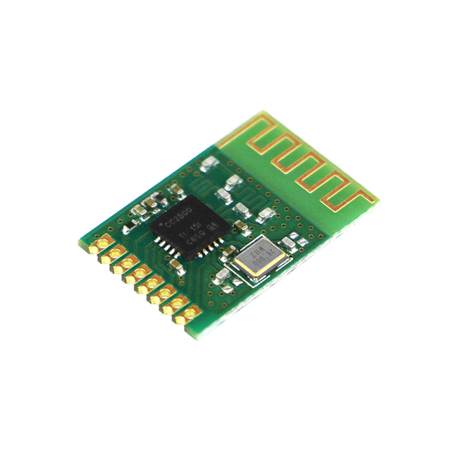
DL-T023-4GW
700~960MHz/1710~2700MHz
1W
| Quantity: | |
|---|---|
4G Spring Coil PCB Antenna with 90° Bent Ending
Antenna Introduction:
Spring coil antenna is a built-in antenna with compact size and simple structure. It has high reliability in various low-power wireless communication applications. The principle of a spring antenna is composed of a folding spring and a matching circuit. The material of our spring antenna is brass, or phosphorous copper, and some will be quipped with a heating shrink tube to prevent oxidation. All are produced from new pure copper materials and can pass the ROHS test. The diameter of the spring and the number of coils are important parameters for controlling the antenna frequency.
The length of each coil is based on /4 units, It is the wavelength of the operating frequency. By increasing the number of coils in the spring, the frequency of the antenna can be reduced, while reducing the number of coils can increase the frequency. The length of a spring antenna is usually multiple of /4, otherwise it will cause reflection and waveform distortion issues. Therefore, when the spring length is not in the case of multiples of /4, a tuning component must be used to match the impedance.
Download Center:
DL-T023-4GW Spring Antenna Specification V1.0 ![]()
Antenna Characteristics:
● REACH/ROSH
● High gain
● Strong compati bility
● Good stability
Application Field:
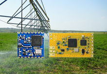
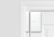
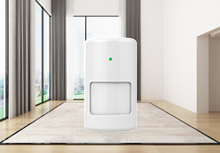
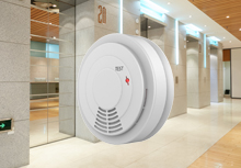
● Smart Express Cabinet
● Security alarm
● Smart buildings, smart buildings
● Smart home
● Power monitoring
● Smart Industry
● Traffic monitoring equipment
● Smart Agriculture
● Temperature and humidity monitor
● Drone
● Medical automation
● Wireless module
Application & Design Guidance :

Note: When making the antenna design, many factors need to be considered, such as the product appearance structure, the position of the RF module’s signal input and output interface, the location of interference sources inside the product, etc. After taking all these factors into consideration, we can then determine the antenna location, angle, distance from the paved ground, and height from the PCB substrate.
Please reserve a π-type network to match the antenna. When debugging the antenna, be sure to provide a complete product shell and internal PCBA function board, calculate the external interference source and parasitic capacitance into the matching, so that the antenna can achieve the best performance indicators and work efficiency.
The PCB trace of the matching network refers to the 0.5mm line width, and the grounding on both sides of the network refers to the 0.35mm spacing to maintain good impedance characteristics.
Electrical Test Report:
| Frequency | 700-960/1710-2700MHz |
| Impedance | 50Ω |
| V.S.W.R | ≦1.5 |
| Band Width | 140/990MHz |
| Gain | 3dBi |
| Linear polarization | Vertical |
| Power | 1W |
| Material | Phosphor bronze; Gold-plated |
| Operating temperature | -40 ~ +85 °C |
| Storage temperature | -40 ~ +85℃ |
4G Spring Coil PCB Antenna with 90° Bent Ending
Antenna Introduction:
Spring coil antenna is a built-in antenna with compact size and simple structure. It has high reliability in various low-power wireless communication applications. The principle of a spring antenna is composed of a folding spring and a matching circuit. The material of our spring antenna is brass, or phosphorous copper, and some will be quipped with a heating shrink tube to prevent oxidation. All are produced from new pure copper materials and can pass the ROHS test. The diameter of the spring and the number of coils are important parameters for controlling the antenna frequency.
The length of each coil is based on /4 units, It is the wavelength of the operating frequency. By increasing the number of coils in the spring, the frequency of the antenna can be reduced, while reducing the number of coils can increase the frequency. The length of a spring antenna is usually multiple of /4, otherwise it will cause reflection and waveform distortion issues. Therefore, when the spring length is not in the case of multiples of /4, a tuning component must be used to match the impedance.
Download Center:
DL-T023-4GW Spring Antenna Specification V1.0 ![]()
Antenna Characteristics:
● REACH/ROSH
● High gain
● Strong compati bility
● Good stability
Application Field:
● Smart Express Cabinet
● Security alarm
● Smart buildings, smart buildings
● Smart home
● Power monitoring
● Smart Industry
● Traffic monitoring equipment
● Smart Agriculture
● Temperature and humidity monitor
● Drone
● Medical automation
● Wireless module
Application & Design Guidance :
Note: When making the antenna design, many factors need to be considered, such as the product appearance structure, the position of the RF module’s signal input and output interface, the location of interference sources inside the product, etc. After taking all these factors into consideration, we can then determine the antenna location, angle, distance from the paved ground, and height from the PCB substrate.
Please reserve a π-type network to match the antenna. When debugging the antenna, be sure to provide a complete product shell and internal PCBA function board, calculate the external interference source and parasitic capacitance into the matching, so that the antenna can achieve the best performance indicators and work efficiency.
The PCB trace of the matching network refers to the 0.5mm line width, and the grounding on both sides of the network refers to the 0.35mm spacing to maintain good impedance characteristics.
Electrical Test Report:
| Frequency | 700-960/1710-2700MHz |
| Impedance | 50Ω |
| V.S.W.R | ≦1.5 |
| Band Width | 140/990MHz |
| Gain | 3dBi |
| Linear polarization | Vertical |
| Power | 1W |
| Material | Phosphor bronze; Gold-plated |
| Operating temperature | -40 ~ +85 °C |
| Storage temperature | -40 ~ +85℃ |