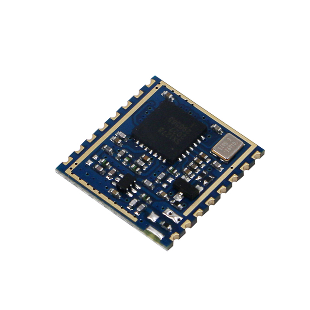


DL-A6601PA-B
DreamLNK
DL-A6601PA-B
433MHz
ARS6601
29.5dBm
3.5~5.3V
-148dBm
6000m
26*20.5*2.8mm
| Availability: | |
|---|---|
| Quantity: | |
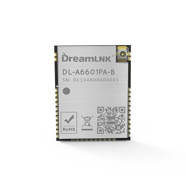
433MHZ/470MHz High-power SOC Wireless LoRa Module with ASR6601 Chip
The DL-A6601PA-B module integrates a Power Amplifier internally, with a maximum TX power of 30dbm, which can effectively improve link budget, thereby improving communication quality and distance. This LoRa module is also equipped with TCXO (Temperature Compensate Crystal Oscillator), which solve the problem of frequency deviation between communication parties caused by the instantaneous heat generated by PA, or the large temperature difference between high and low environments. At the same time, it can also achieve narrower bandwidth at room temperature, with higher sensitivity and stable communication.
As for the RF characteristic, compared to traditional modulation methods, its LORA modulation can greatly improve the RF performance in all aspects. The RX current is 7mA, and the highest sensitivity can reach up to -148dBm.
This LoRa module fully utilizes the ASR6601 chip’s anti-interference ability, its high sensitivity and low power consumption make this RF module excellent in long-range communication, which can be widely used in various wireless communication fields of the IoT industry, especially battery powered application, and long-distance communication projects.
Moreover, this LoRa module has 24 GPIOs, and the RF circuit of this LoRa module has been matched and optimized by professional equipment, which will guarantee its good performance under high power in such compact size. You can easily develop wireless products with stable performance and high reliability base on this RF module, without having a deep understanding of RF circuit design.
Features
● Support multiple modulation methods: LoRa™, FSK, GFSK, MSK, GMSK, OOK,
● Frequency range (chip supported): 137~525MHz;
● Recommended frequency (module itself): 410~510MHz
● The working voltage is 5V, the output power can up to 30dBm (1W), and the maximum instantaneous working current is 640mA.
● Support fast Channel Activity Detection (CAD);
● Low power consumption under receiving state, and the receiving current is 17mA
(with CAD function, it can effectively reduce the overall current consumption, suitable for battery powered applications);
● Sleep current: 1uA;
● Supports fast frequency hopping, CRC hardware verification, and interrupt DIOx mapping;
● Theoretical sensitivity of the chip: -149dBm@LoRa;
● Industrial grade standard design, support long-term use at -30~85 C;
● Spreading factor supported: SF6/SF7/SF8/SF9/SF10/SF11/SF12;
● Bandwidth supported: 7.8/10.4/15.6/20.8/31.25/41.7/62.5/125/250/500kHz;
Applications
● Wireless automatic meter reading (water meter, electric meter, gas meter)
● Ultra-long distance data communication
● Smart home system
● Intelligent security monitoring
● Smart building
● Industrial controllers, sensors
● Agricultural automation solutions
● Intelligent parking system
● Container information management
● Automotive industry applications
● Supply chain logistics
Download Center
DL-A6601PA-B Specification V1.0
Technical Parameter
Parameter | Min. | Typical | Max. | Unit | Remarks |
Operating Conditions | |||||
Working Voltage (VDD) | 3.4 | 3.7 | 5.4 | V | The voltage cannot exceed 5.4V, Otherwise, it may burn out the module |
Communication Level Range | -0.3 | 3.3 | 3.6 | V | Exceeding this range will damage the chip |
Working Temperature Range | -40 | 25 | 85 | ℃ | The larger the temperature difference, the greater the bandwidth required for communication (temperature compensation crystal was equipped) |
Current Consumption | |||||
Receiving Current | 6 | 6.6 | 8 | mA | @MCU+Radio DCDC Software adopts WOR working mode, which can effectively reduce the overall working current |
Transmission Current | 510 | 578 200 | 800 | mA | @433MHz @DCDC @ANT 50-ohm impedance; TX +29.5dbm @ANT 50-ohm impedance; TX +20dbm |
525 | 600 230 | 829 | mA | @868MHz @915MHz @DCDC @ANT 50-ohm impedance; TX +29dbm @ANT 50-ohm impedance; TX +20dbm | |
Max. Current | - | 1.2A | - | A | RF transmission is related to many factors, such as power and antenna matching. What we provided are the requirements that need to be met when designing power supplies |
Sleep Current | 3 | 3.5 | 5 | uA | Save via register |
RF Parameters | |||||
Recommended Frequency (For best performance) | 400 | 433/470 | 510 | MHz | @433MHz/470Mhz RF module |
820 | 868/915 | 960 | MHz | @868MHz/915Mhz RF module | |
Transmit Power Range | -10 | 20 | 20 | dBm | Software configurable |
LORA Receiving sensitivity | -143 | dBm | @DR= 0.067Kbps, BW_L = 15.6kHz, SF = 11 | ||
-130 | dBm | @DR= 1.758Kbps, BW_L= 125KHz, SF=9 | |||
-120 | dBm | @DR= 10.94Kbps, BW_L = 250kHz, SF = 7 | |||
FSK Receiving sensitivity | -123 | dBm | @DR=1.2Kbps, FDA = 0.8 kHz, BW_F= 4 kHz | ||
-109 | dBm | @DR=38.4Kbps, FDA = 40 kHz, BW_F=160kHz | |||
-104 | dBm | @DR=250Kbps, FDA =125 kHz, BW_F=500 kHz | |||
LoRa Payload Rate | 0.018 | - | 62.5 | Kb/s | For application with low transmission rate |
FSK Rate Range | 0.6 | - | 300 | Kb/s | For application with high transmission rate |
Product Size:
Pin Diagram:
No | Definitions | Type | Description |
1 | VDD | PWR | Powered by 5.5V-3.4V, and passes through a 3.3V LDO internally |
2 | GND | PWR | Reliable grounding |
3 | PA1 | IO | Universal GPIO / Serial Port Download; TXD |
4 | PA0 | IO | Universal GPIO / Serial Port Download; RXD |
5 | PA3 | IO | Universal GPIO port |
6 | PA2 | IO | Universal GPIO / Enter serial port for download PA2, power on and pull high to enter download mode |
7 | PA6 | IO | Universal GPIO / SWDAT download and debugging port |
8 | PA7 | IO | Universal GPIO / SWDCLK download and debugging port |
9 | PB0 | IO | Universal GPIO / UART0_RXD |
10 | PB1 | IO | Universal GPIO / UART0_TXD |
11 | PA14 | IO | Universal GPIO port |
12 | PA15 | IO | Universal GPIO port |
13 | PD14 | IO | Universal GPIO port |
14 | PD12 | IO | Universal GPIO port |
15 | RSTN | I | Reset pin, effective at low level |
16 | PA11 | IO | Universal GPIO port |
17 | PA8 | IO | Universal GPIO port |
18 | PA5 | IO | Universal GPIO port |
19 | PA4 | IO | Universal GPIO port |
20 | PD10 | IO | Universal GPIO port |
21 | NC/3V3 | NC | Internal LDO, 3.3V, normally can be “floating” |
22 | NC | NC | No connection |
23 | PA9 | IO | Universal GPIO port |
24 | PC15 | IO | Universal GPIO port |
25 | PC13 | IO | Universal GPIO port |
26 | PC12 | IO | Universal GPIO port |
27 | NC | NC | No connection |
28 | PC5 | IO | Universal GPIO port |
29 | PC1 | IO | Universal GPIO port |
30 | PC0 | IO | Universal GPIO port |
31 | NC | NC | No connection |
32 | NC | NC | No connection |
33 | GND | PWR | Reliable grounding |
34 | ANT | AI/IO | RF signal input/output port, π-matching circuit must be reserved; Adopt 50Ω impedance matching for RF routing, route the ground and add via holes around it |
35 | GND | PWR | Reliable grounding |
36 | GND | PWR | Reliable grounding |
DreamLNK is a high-tech enterprise specializing in ISM band micropower wireless communication technology, providing different kinds of wireless modules and one-stop IoT solutions, including 433/868/915MHz wireless modules, 2.4G wireless Modules, FSK Transceiver Modules, LoRa Modules, Antennas, Remote Controls, and customized wireless RF solutions. Welcome to inquire!
