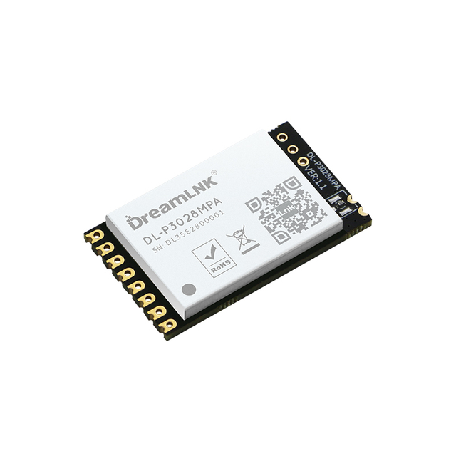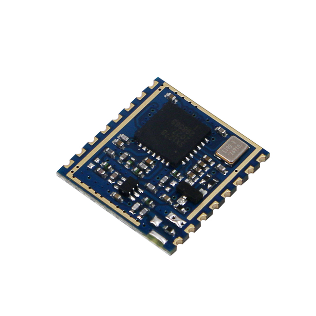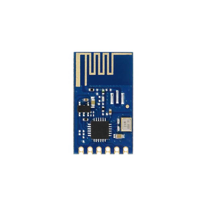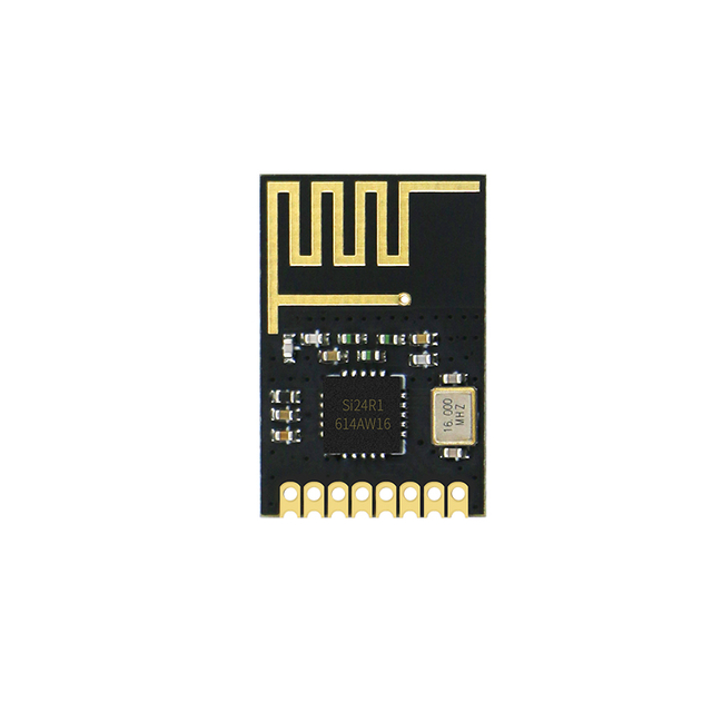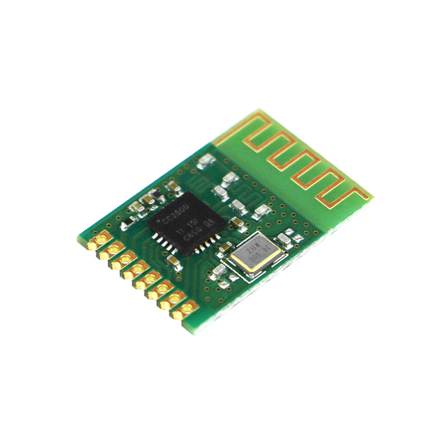


DL-A7149K8
DreamLNK/骏晔科技
DL-A7149K8
433/868/915mhz
AMICCOM A7149
2.2~3.6V
800M
20.1*12*2mm
| Availability: | |
|---|---|
| Quantity: | |
Brief Introduction
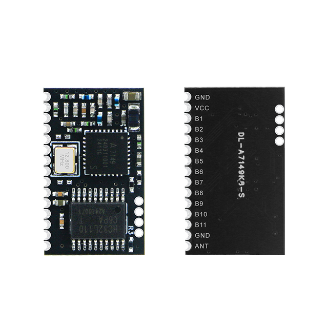
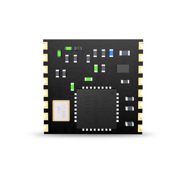
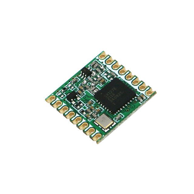
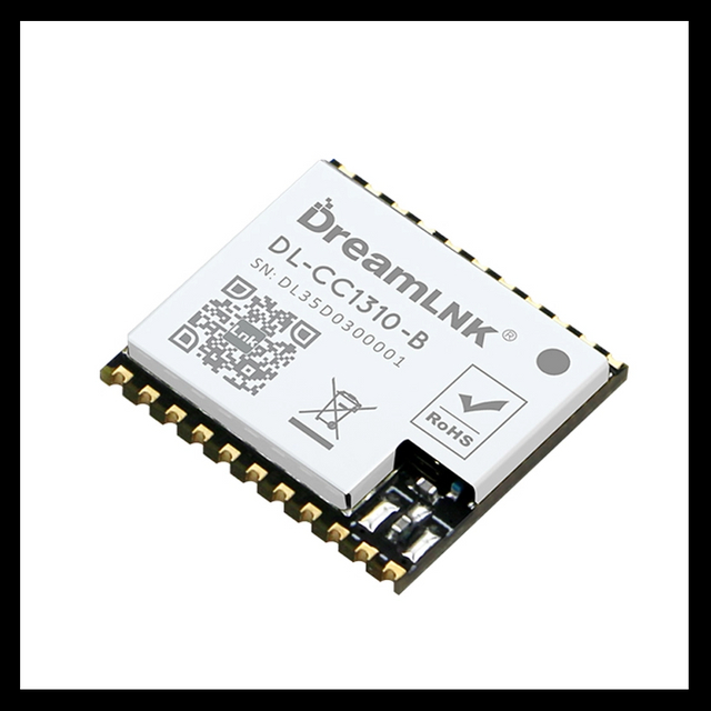
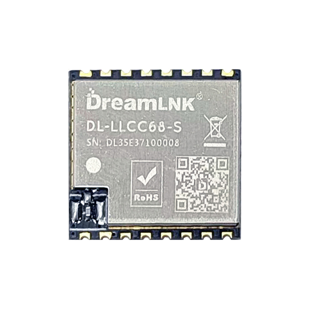
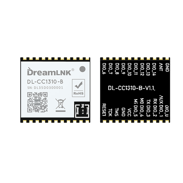
The DL-A7149K8 Wireless Module is a cost-effective, compact size, high sensitivity, long-range, 8-channel Switching FSK Transceiver Module developed by DreamLNK. It is no need to design complex underlying driver software, also no need to define the transceiver communication protocol, nor the key value definition. With pre-optimized code matching, remote control, low power consumption, and co-frequency Interference capability, you just need to connect the necessary input buttons and output loads, code matching button, code matching indicator, etc. Then it can be used without any programming.
There are 2 versions DL-A7149K8 RF modules, the DL-A7149K8-TX one is a transmitter module, while DL-A7149K8-RX version is the receiver module. After triggering, the TX module automatically enters sleep mode, while the RX module has normal mode and WoR (low-power) mode, which were specifically designed for battery powered systems to achieve wireless receiving functionality and low-power requirements.
These Switching RF Modules can be triggered by high and low levels: after the transmission mode button is triggered, the corresponding output port of the receiver module can output a level signal. The standard Digital RF Module has 8 independent control signals. The 8 buttons on the transmitter correspond to the 8 signal outputs of the receiver module. It can realize single-channel remote control, as well as multi-channels remote control simultaneously.
This Wireless Module is compact in size, low in power consumption, and easy to use. The transmitter module only needs to design the key board according to the remote-control shell. The receiver module has no peripheral parts. The signal of the I/O ports can directly drive small loads such as LEDs, motors, and relays. These 8 output signals can also be provided as parallel level signals to the I/O port of the MCU for use. It is very convenient and simple to use, and multiple sets of products can be used simultaneously without interfering with each other.
Features
● Frequency Bands: 433Mhz/868MHz/915MHz;
● RX can choose between normal mode and WOR mode to reduce the average receiving current;
● It adopts code hopping and random frequency allocation to reduce the risk of fixed frequency interference;
● Highly integrated, small size, ultra-low power design, suitable for low-power application scenarios;
● Support multi-ID storage, the receiver module can store up to 20 different IDs, making it easy to manage the access and control of multiple transmitting devices;
● Multi-channel independent control, 8-channel switch output, support single or multiple channel simultaneous control, can meet complex remote-control requirements;
● Easy to use, no programming required, users only need to connect the required peripheral devices such as buttons and loads to use.
Download Center
DL-A7149K8 Specification (data sheet) V1.0
Typical Application
● Multi-channel controller for electric vehicles
● Multi-channel input and output switch control
● Multi-channel lighting fixtures remote control
● AMR system (Wireless meter reading)
● Wireless multi-channel opening and closing controller
● Multi-channel level control circuit
● Smart buildings, Smart home
● Intelligent Switch
Technical Parameter
Parameter | Min. | Typical | Max. | Unit | Remarks |
Operating Conditions | |||||
Working Voltage | 2.2 | 3.3 | 3.6 | V | To ensure maximum chip power, stable voltage should ≥ 3.2V |
Communication Level Range | -0.3 | 3.3 | 3.6 | V | Out range may damage the chip |
Working Temperature Range | -40 | 25 | 85 | ℃ | The larger the temperature difference, the greater the required bandwidth |
Current Consumption | |||||
Receiving Current @ Normal Mode | 2.5 | 3.5 | 4.2 | mA | WoR mode can effectively reduce the overall working current |
WOR Mode (Low Power Mode) | 100 | uA | In WoR mode, RX wake-up detection is performed once every 500mS, with an average standby current of about 100uA (sleep time can be customized, and the longer the sleep time, the lower the power consumption) | ||
TX Current | 87 | 107 | 127 | mA | @433MHz 19dBm |
78 | 98 | 118 | mA | @868MHz/915MHz 17dBm | |
Sleep Current | 2.5 | uA | |||
RF Parameters | |||||
Transmitting Power | 19 | dBm | 433M | ||
17 | dBm | 868/915M | |||
Receiving Sensitivity | -115 -113 -111 | dBm | @433MHz,10Kbps, IFBW:50KHz @868MHz,10Kbps, IFBW:50KHz @915MHz,10Kbps, IFBW:50KHz | ||
Pin Definitions
DL-A7149K8-TX Pins Definitions
Pin No | Pin’s Name | Type | Description |
1 | GND | PWR | Reliable grounding |
2 | VCC | PWR | Power supply |
3 | B1~B8 | I | 8-channel data pin, Low level trigger, transmit button active (When TX at low level, RX will at high level) |
4 | B9 | I | Low level trigger, enters code pairing state |
5 | B10 | I | Indicator pin (code matching, transmitting status), for LED connecting |
6 | B11 | I | High level uses 4Byte preamble, low level uses 64Byte preamble (Long preamble can effectively WoR low-power mode) Note: long preamble also takes a long time to send |
7 | VCC | PWR | 3.3V |
8 | ANT/NC | AI/AO | Analog antenna Input/output interface, 50Ω impedance, make it grounded, and add via holes |
DL-A7149K8-RX Pins Definitions
Pin No | Pin’s Name | Type | Description |
1 | GND | PWR | Reliable grounding |
2 | VCC | PWR | Power supply |
3 | B1~B8 | O | 8-channel data pin, Low level trigger, transmit button active (When TX at low level, RX will at high level) |
4 | B9 | I | Low level trigger, enters code pairing state |
5 | B10 | I | Indicator pin (code matching, transmitting status), for LED connecting |
6 | B11 | I | Output mode selection. Set low level (0) for Latch Mode, set high level (1) for Inching Mode (momentary control) |
7 | GND | PWR | Reliable grounding |
8 | ANT/NC | AI/AO | Analog antenna Input/output interface, 50Ω impedance, make it grounded, and add via holes |
Module Size
Product Tags
RF module, Wireless Module, Wireless Transmitter Module, RF Transmitter Module, 433MHz RF Module, Wireless Transceiver Module, FSK Transceiver module, 433MHz Wireless module, 868MHz Wireless module, 915MHz Wireless module, UART Module, Switch Control RF Module
