|


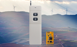
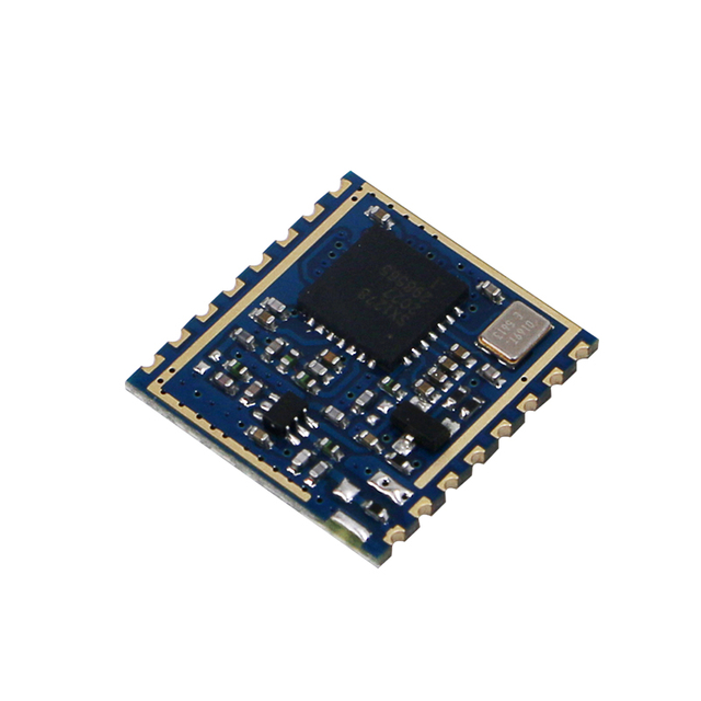
DL-A7149-S
DreamLNK/骏晔科技
DL-A7149-S
433MHz/868MHz/915MHz
AMICCOM A7149
-30~20dBm
2.2~3.6V
-119dBm
1000m
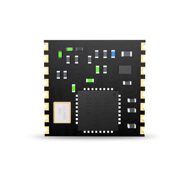
12.5*12*2mm
| Quantity: | |
|---|---|
Ultra-low Power Consumption FSK Transceiver Module with Amiccom A7149 chip

Brief Introduction
DL-A7149-S was designed base on AMICCOM A7149 wireless transceiver chip. It is a compact and low power RF transceiver module. This AMICCOM A7149 is an ISM band wireless transceiver chip, mainly set to 433/868/915/MHz ISM/SRD frequency bands, with very low power consumption (e.g.: power consumption under 434MHz band in RX mode is just 1.8mA @ AGC Off).
Its link budget is very high, making it ideal for battery-powered long-distance wireless transmission applications. Its efficient Class E amplifier has an output power of up to 20dBm, a Max. sensitivity of -119dBm, and a Max. transmission rate of 250Kbps. By using this RF module, you can easily develop an excellent wireless product, with good RF performance and high reliability, without having a deep understanding of RF circuit design.
Features
● Compact size, SMD stamp edge half-hole encapsulation;
● Modulation method: FSK/GFSK;
● Working Voltage: 2.2~3.6V;
● Operating Frequency: 433MHz/868MHz/915MHz;
● Chip support speed range: 2-250Kbps;
● Low power consumption, receiving current 1.8mA (AGC Off);
● The maximum output power reaches 20dBm;
● High receiving sensitivity: -119dBm@2kbps;
● Independent 64BYTE transmit/receive data buffer;
● To reduce the power consumption, switching time between standby and receive state can be set (WOR function);
● Supports RSSI signal strength detection.
Highlight Advantages:
Ultra-low Power Consumption (with only 1.8mA at full receiving state, best for battery powered applications)
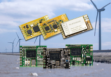
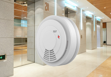
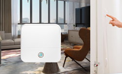
At present, the power consumption of FSK transceiver chips in 433/868/915Mhz IoT applications is around 10mA, which cannot meet the requirements of most systems in industrial control and data acquisition industries, as most of them use battery power and require 3-5 years of use. But this DL-A7149-S RF module can achieve excellent power planning through software algorithm optimization, by optimizing the receiving working current to 1.8mA, extremely suitable for battery powered applications that require a long-life cycle, such as AMR (heat meters, gas meters, electricity meter, etc.), Remote Anti-theft Devices, Industrial Control, Smart Buildings, Energy Management, Smart Homes, Smart Security, Smart Agriculture, etc.

Wake on Radio (WOR): switching time between standby and receiving state can be set to reduce power consumption
By reducing the receiving state time of the receiver (while the rest of the time operates in deep sleep mode), the overall power consumption of the device can be reduced while ensuring its normal working.
Power Management:
Supports Deep Sleep Mode, Sleep, Idle Mode, and WOR Mode (Wake on Radio). The WOR function provides A7149 with automatic wake-up to receive RF network packets at irregular intervals. When it enters Deep Sleep Mode, it only consumes a current of 40nA. Overall, A7149 is a new generation of high-performance RF IC with extremely low receiving current and built-in +20dBm power amplifier, providing extremely long transmission range. The built-in power management function can greatly extend the battery life.

Other Advantages:
1. RSSI (Received Signal Strength Indication)
Built in RSSI can help you in detecting clean transmission channels, and the Auto Calibration mechanism inside the IC is used to overcome variations in semiconductor processes and work stably in various environments.

2. AFC (Automatic Frequency Compensation)
The function of Automatic Frequency Compensation (AFC) can solve the sensitivity degradation caused by RF frequency offset.
3. Ultra Long Range
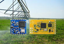
Sub-1Ghz long-distance wireless module, can achieve 1KM communication range in an open space (without interference).
4. -120dBm High Receiving Sensitivity
High receiving sensitivity -120dBm@2Kbps, IFBW:50khz
5. Ultra Compact Size
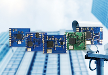
Ultra small packaging surface mount design: 12.5*12mm (only half the size of a coin).
Applications
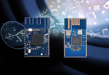
● ISM band data communication ;
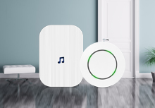
● Smart Building;
● Smart Home System ;
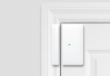
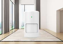
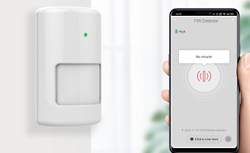
● Intelligent Security Monitoring ;
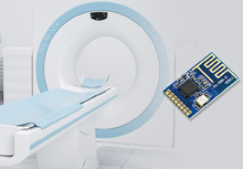
● AMR (Automatic Mobile Robot) ;
● Wireless Remote Control;
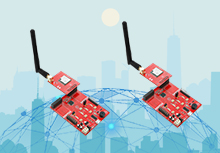
● Wireless Sensor Networking ;
● Energy Control and Management ;
● RKE (Remote Keyless Entry) ;
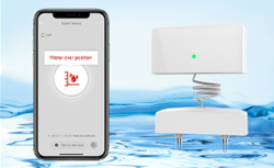
● Heat energy collection, meter measurement ;
Download Center
DL-A7149-S FSK Wireless Transceiver Module - V1.0.pdf ![]()
Technical Parameter
Parameter | Min. | Typical | Max. | Unit | Remarks |
Operating Conditions | |||||
Working Voltage (VDD) | 2.2 | 3.3 | 3.6 | V | To ensure maximum chip power, stable voltage should ≥3.1V |
Communication Level Range | -0.3 | 3.3 | 3.6 | V | Exceeding this range will damage the chip |
Working Temperature Range | -40 | 25 | 85 | ℃ | The larger the temperature difference, the greater the bandwidth is required for communication |
Current Consumption | |||||
Receiving Current | 1.8 | 2.2 | 3.8 | mA | @DCDC WOR working mode can be used to reduce the overall working current |
Transmission Current | 97 | 117 | 137 | mA | @433MHz: 19dBm, DCDC 50Ω |
78 | 98 | 118 | mA | @868MHz/915MHz: 17dBm, DCDC 50Ω | |
Sleep Current | 0.2 | 0.5 | 1 | uA | Save via register |
RF Parameters | |||||
Transmit Power Range | -30 | 19 | 20 | dBm | Software configurable |
Receiving Sensitivity | -119 -117 -115 | dBm | @433MHz,2Kbps, IFBW:50KHz @868MHz,2Kbps, IFBW:50KHz @915MHz,2Kbps, IFBW:50KHz | ||
Communication Rate Range | 2 | 100 | Kb/s | @Different crystals result in varying rates, Max. up to 250K | |
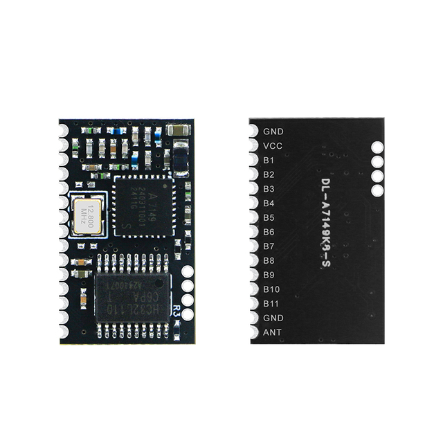
Pins Definition

No | Definitions | Type | Description |
1 | ANT/NC | AI/AO | RF signal input/output port, π-matching circuit must be reserved; Adopt 50Ω impedance matching for RF routing, route the ground and add via holes around it |
2 | GND | PWR | Reliable grounding |
3 | 3.3V | PWR | To ensure maximum chip performance, a stable voltage (≥3.1V) is required |
4 | GPIO2 | O | Function can be configured through the SPI interface |
5 | GIO1 | O | Function can be configured through the SPI interface |
6 | SDIO | IO | SPI data input/outpu |
7 | SCK | I | SPI Serial Clock Input, connected to the SCLK of MCU |
8 | SCS | I | SPI Chip Select Input, connected to the CSN of MCU |
9 | GND | PWR | Reliable grounding |
10 | NC | NA | No connection |
11 | NC | NA | No connection |
12 | PDNHA | I | DC-DC PWM mode control, high level for sleeping |
13 | NC | NA | No connection |
14 | RST | I | Hardware reset to increase its stability, chip initialization, low-level reset |
15 | CKO | O | SPI Serial Clock output, no connection is needed |
16 | GND | PWR | Reliable grounding |
Size![]()

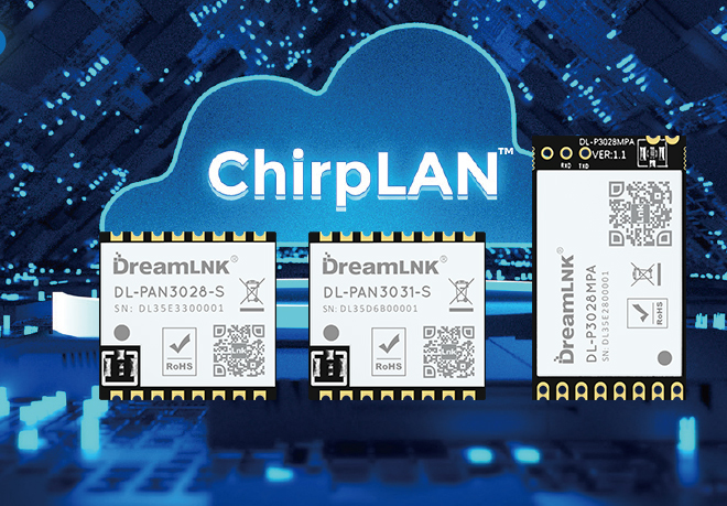
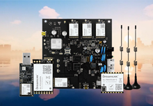
DreamLNK is a high-tech enterprise specializing in ISM band micropower wireless communication technology, providing different kinds of wireless modules and one-stop IoT solutions, including 433/868/915MHz wireless modules, 2.4G RF Modules, FSK Transceiver Modules, Antennas, Remote Controls, and customized wireless RF solutions. Welcome to inquire!
Ultra-low Power Consumption FSK Transceiver Module with Amiccom A7149 chip
Brief Introduction
DL-A7149-S was designed base on AMICCOM A7149 wireless transceiver chip. It is a compact and low power RF transceiver module. This AMICCOM A7149 is an ISM band wireless transceiver chip, mainly set to 433/868/915/MHz ISM/SRD frequency bands, with very low power consumption (e.g.: power consumption under 434MHz band in RX mode is just 1.8mA @ AGC Off).
Its link budget is very high, making it ideal for battery-powered long-distance wireless transmission applications. Its efficient Class E amplifier has an output power of up to 20dBm, a Max. sensitivity of -119dBm, and a Max. transmission rate of 250Kbps. By using this RF module, you can easily develop an excellent wireless product, with good RF performance and high reliability, without having a deep understanding of RF circuit design.
Features
● Compact size, SMD stamp edge half-hole encapsulation;
● Modulation method: FSK/GFSK;
● Working Voltage: 2.2~3.6V;
● Operating Frequency: 433MHz/868MHz/915MHz;
● Chip support speed range: 2-250Kbps;
● Low power consumption, receiving current 1.8mA (AGC Off);
● The maximum output power reaches 20dBm;
● High receiving sensitivity: -119dBm@2kbps;
● Independent 64BYTE transmit/receive data buffer;
● To reduce the power consumption, switching time between standby and receive state can be set (WOR function);
● Supports RSSI signal strength detection.
Highlight Advantages:
Ultra-low Power Consumption (with only 1.8mA at full receiving state, best for battery powered applications)
At present, the power consumption of FSK transceiver chips in 433/868/915Mhz IoT applications is around 10mA, which cannot meet the requirements of most systems in industrial control and data acquisition industries, as most of them use battery power and require 3-5 years of use. But this DL-A7149-S RF module can achieve excellent power planning through software algorithm optimization, by optimizing the receiving working current to 1.8mA, extremely suitable for battery powered applications that require a long-life cycle, such as AMR (heat meters, gas meters, electricity meter, etc.), Remote Anti-theft Devices, Industrial Control, Smart Buildings, Energy Management, Smart Homes, Smart Security, Smart Agriculture, etc.
Wake on Radio (WOR): switching time between standby and receiving state can be set to reduce power consumption
By reducing the receiving state time of the receiver (while the rest of the time operates in deep sleep mode), the overall power consumption of the device can be reduced while ensuring its normal working.
Power Management:
Supports Deep Sleep Mode, Sleep, Idle Mode, and WOR Mode (Wake on Radio). The WOR function provides A7149 with automatic wake-up to receive RF network packets at irregular intervals. When it enters Deep Sleep Mode, it only consumes a current of 40nA. Overall, A7149 is a new generation of high-performance RF IC with extremely low receiving current and built-in +20dBm power amplifier, providing extremely long transmission range. The built-in power management function can greatly extend the battery life.
Other Advantages:
1. RSSI (Received Signal Strength Indication)
Built in RSSI can help you in detecting clean transmission channels, and the Auto Calibration mechanism inside the IC is used to overcome variations in semiconductor processes and work stably in various environments.
2. AFC (Automatic Frequency Compensation)
The function of Automatic Frequency Compensation (AFC) can solve the sensitivity degradation caused by RF frequency offset.
3. Ultra Long Range
Sub-1Ghz long-distance wireless module, can achieve 1KM communication range in an open space (without interference).
4. -120dBm High Receiving Sensitivity
High receiving sensitivity -120dBm@2Kbps, IFBW:50khz
5. Ultra Compact Size
Ultra small packaging surface mount design: 12.5*12mm (only half the size of a coin).
Applications
● ISM band data communication ;
● Smart Building;
● Smart Home System ;
● Intelligent Security Monitoring ;
● AMR (Automatic Mobile Robot) ;
● Wireless Remote Control;
● Wireless Sensor Networking ;
● Energy Control and Management ;
● RKE (Remote Keyless Entry) ;
● Heat energy collection, meter measurement ;
Download Center
DL-A7149-S FSK Wireless Transceiver Module - V1.0.pdf ![]()
Technical Parameter
Parameter | Min. | Typical | Max. | Unit | Remarks |
Operating Conditions | |||||
Working Voltage (VDD) | 2.2 | 3.3 | 3.6 | V | To ensure maximum chip power, stable voltage should ≥3.1V |
Communication Level Range | -0.3 | 3.3 | 3.6 | V | Exceeding this range will damage the chip |
Working Temperature Range | -40 | 25 | 85 | ℃ | The larger the temperature difference, the greater the bandwidth is required for communication |
Current Consumption | |||||
Receiving Current | 1.8 | 2.2 | 3.8 | mA | @DCDC WOR working mode can be used to reduce the overall working current |
Transmission Current | 97 | 117 | 137 | mA | @433MHz: 19dBm, DCDC 50Ω |
78 | 98 | 118 | mA | @868MHz/915MHz: 17dBm, DCDC 50Ω | |
Sleep Current | 0.2 | 0.5 | 1 | uA | Save via register |
RF Parameters | |||||
Transmit Power Range | -30 | 19 | 20 | dBm | Software configurable |
Receiving Sensitivity | -119 -117 -115 | dBm | @433MHz,2Kbps, IFBW:50KHz @868MHz,2Kbps, IFBW:50KHz @915MHz,2Kbps, IFBW:50KHz | ||
Communication Rate Range | 2 | 100 | Kb/s | @Different crystals result in varying rates, Max. up to 250K | |
Pins Definition
No | Definitions | Type | Description |
1 | ANT/NC | AI/AO | RF signal input/output port, π-matching circuit must be reserved; Adopt 50Ω impedance matching for RF routing, route the ground and add via holes around it |
2 | GND | PWR | Reliable grounding |
3 | 3.3V | PWR | To ensure maximum chip performance, a stable voltage (≥3.1V) is required |
4 | GPIO2 | O | Function can be configured through the SPI interface |
5 | GIO1 | O | Function can be configured through the SPI interface |
6 | SDIO | IO | SPI data input/outpu |
7 | SCK | I | SPI Serial Clock Input, connected to the SCLK of MCU |
8 | SCS | I | SPI Chip Select Input, connected to the CSN of MCU |
9 | GND | PWR | Reliable grounding |
10 | NC | NA | No connection |
11 | NC | NA | No connection |
12 | PDNHA | I | DC-DC PWM mode control, high level for sleeping |
13 | NC | NA | No connection |
14 | RST | I | Hardware reset to increase its stability, chip initialization, low-level reset |
15 | CKO | O | SPI Serial Clock output, no connection is needed |
16 | GND | PWR | Reliable grounding |
Size![]()
DreamLNK is a high-tech enterprise specializing in ISM band micropower wireless communication technology, providing different kinds of wireless modules and one-stop IoT solutions, including 433/868/915MHz wireless modules, 2.4G RF Modules, FSK Transceiver Modules, Antennas, Remote Controls, and customized wireless RF solutions. Welcome to inquire!