|


RFM23BP
433/470/868/915MHz
RFM23BP
30dBm
1.8V-3.6V
-120 dBm
2000m
33x18x2 mm
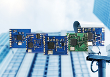
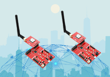
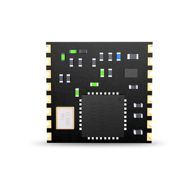
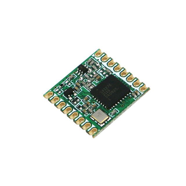
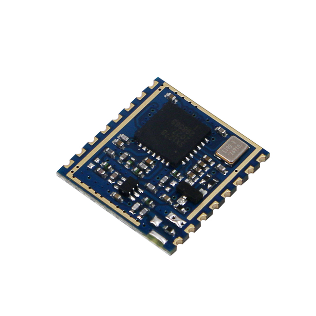
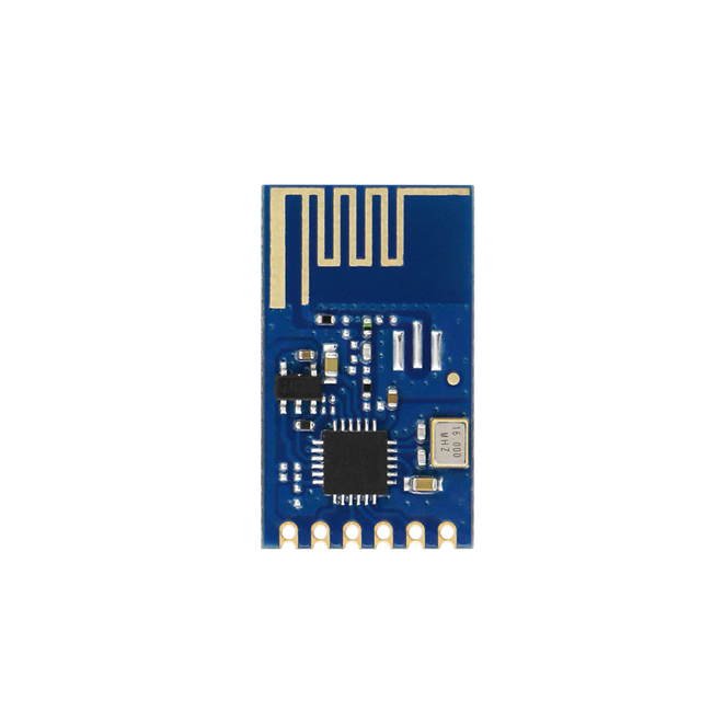
FSK Two-way RF Transceiver Module RFM23BP
RFM23BP are highly integrated, low cost,433/868/915MHZ wireless transceivers module. The low receive sensitivity (–120dBm) coupled with industry leading +30dBm output power ensures extended range and improved link performance. Built-in antenna diversity and support for frequency hopping can be used to further extend range and enhance performance.
Additional system features such as an automatic wake-up timer, low battery detector, 64 byte TX/RX FIFOs, automatic packet handling, and preamble detection reduce overall current consumption and allow the use of lower-cost system MCUs. An integrated temperature sensor, general purpose ADC, power-on-reset (POR), and GPIOs further reduce overall system cost and size.
The RFM23BP digital receive archit ecture features a high-performance ADC and DSP based modem which performs demodulation, filtering, and packet handling for increased flexibility and performance. The direct digital transmit modulation and automatic PA power ramping ensure precise transmit modulation and reduced spectral spreading ensuring compliance with global regulations including FCC, ETSI.
An easy-to-use calculator is provided to quickly configure the radio settings,simplifying customer's system design and reducing time to market.
Features
● Frequency Range: 433/868/915MHz ISM bands
● Sensitivity: –120 dBm
● Output power range: +30 dBm Max (RFM23BP)
● Low Power Consumption:
25mA in receive state
550 mA @ +30dBm transmit
● Transmission Rate: 0.123 to 256 kbps
● FSK, GFSK, and OOK modulation
● Power Supply: 3.3 to 6 V
● Ultra low power shutdown mode
● Digital RSSI
● Wake-up timer
● Auto-frequency calibration (AFC)
● Power-on-reset (POR)
● Antenna diversity and TR switch control
● Configurable packet handler
● Preamble detector
● TX and RX 64 byte FIFOs
● Low battery detector
● Temperature sensor and 8-bit ADC
● –40 to +85 °C temperature range
● Integrated voltage regulators
● Frequency hopping capability
● On-chip crystal tuning
● 16-PIN SMD package
● Low cost
Applications
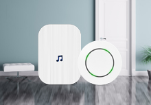
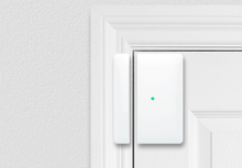
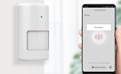
● Remote control
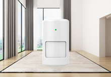
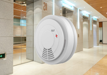
● Home security & alarm
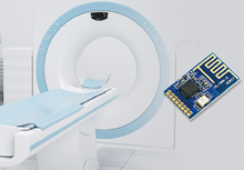
● Telemetry
● Personal data logging
● Toy control
● Tire pressure monitoring
● Wireless PC peripherals
● Remote meter reading
● Remote keyless entry
● Home automation
● Industrial control
● Sensor networks
● Health monitors
● Tag readers
Download Center
Electrical Specifications
DC characteristics
| Parameter | Symbol | Conditions | Min | Typ | Max | Units |
| Supply Voltage Range | VDD | 3.3 | 5 | 6 | V | |
| Power Saving Modes | I Shutdown | RC Oscillator, Main Digital Regulator, and Low Power Digital Regulator OFF | - | 15 | 50 | nA |
| I Standby | Low Power Digital Regulator ON (Register values retained) and Main Digital Regulator, and RC Oscillator OFF | - | 450 | 800 | nA | |
| I Sleep | RC Oscillator and Low Power Digital Regulator ON (Register values retained) and Main Digital Regulator OFF | - | 1 | - | µA | |
| I Sensor-LBD | Main Digital Regulator and Low Battery Detector ON, Crystal Oscillator and all other blocks OFF | - | 1 | - | µA | |
| I Sensor-TS | Main Digital Regulator and Temperature Sensor ON, Crystal Oscillator and all other blocks OFF | - | 1 | - | µA | |
| I Ready | Crystal Oscillator and Main Digital Regulator ON, all other blocks OFF. Crystal Oscillator buffer disabled | - | 800 | - | µA | |
| TUNE Mode Current | I Tune | Synthesizer and regulators enabled | - | 8.5 | - | mA |
| RX Mode Current | I RX | - | 25 | - | mA | |
TX Mode Current —RFM23BP | I TX_+Max | txpow[2:0] = 110 (+30 dBm) | - | 550 | - | mA |
| I TX_+Min | txpow[2:0] = 001 (TBD dBm) | - | TBD | - | mA |
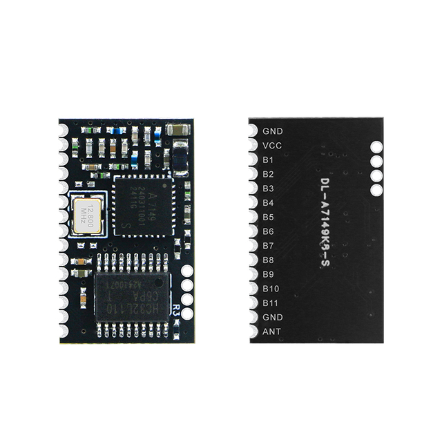
Pins Definition

| VCC | S | +3.3 to +6 V supply voltage. The recommended V CC supply voltage is +5V. |
| GND | S | Ground reference. |
| GPIO_0 | I/O | General Purpose Digital I/O that may be configured through the registers to perform various functions including: Microcontroller Clock Output, FIFO status, POR, Wake-Up timer, Low Battery Detect, TRSW, AntDiversity control, etc. See the SPI GPIO Configuration Registers, Address 0Bh, 0Ch, and 0Dh for more information. |
| GPIO_1 | I/O | |
| GPIO_2 | I/O | |
| SDO | O | 0–V CC V digital output that provides a serial readback function of the internal control registers. |
| SDI | I | Serial Data input. 0–V CC V digital input. This pin provides the serial data stream for the 4-line serial data bus. |
| SCLK | I | Serial Clock input. 0–V DD V digital input. This pin provides the serial data clock function for the 4-line serial data bus. Data is clocked into the RFM23PS on positive edge transitions. |
| nSEL | I | Serial Interface Select input. 0– V CC V digital input. This pin provides the Select/Enable function for the 4-line serial data bus. The signal is also used to signify burst read/write mode. |
| nIRQ | O | General Microcontroller Interrupt Status output. When the RFM23PS exhibits anyone of the Interrupt Events the nIRQ pin will be set low=0. Please see the Control Logic registers section for more information on the Interrupt Events. The Microcontroller can then determine the state of the interrupt by reading a corresponding SPI Interrupt Status Registers, Address 03h and 04h. |
| SDN | I | Shutdown input pin. 0–V CC V digital input. SDN should be = 0 in all modes except Shutdown mode. When SDN =1 the chip will be completely shutdown and the contents of the registers will be lost. |
| TX_ON | I | Tx ON select input pin, When RFM23BP is TX state,TX_ON should be = 0, RX_ON should be = 1 |
| RX_ON | I | Rx ON select input pin, When RFM2 3BPS is RX state,RX_ON should be = 0, TX_ON should be = 1 |
| ANT | I/O | RF signal output/input.(50 OHM output /input Impedance |
Size

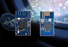
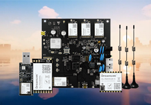
Dreamlnk is a high-tech enterprise specializing in ISM band micropower wireless communication technology, providing different kinds of wireless modules and one-stop IoT solutions, including 433/868/915MHz wireless modules, 2.4G wireless Modules, FSK Wireless Transceiver Modules, Antennas, Remote Controls, and customized wireless RF solutions. Welcome to inquire!
FSK Two-way RF Transceiver Module RFM23BP
RFM23BP are highly integrated, low cost,433/868/915MHZ wireless transceivers module. The low receive sensitivity (–120dBm) coupled with industry leading +30dBm output power ensures extended range and improved link performance. Built-in antenna diversity and support for frequency hopping can be used to further extend range and enhance performance.
Additional system features such as an automatic wake-up timer, low battery detector, 64 byte TX/RX FIFOs, automatic packet handling, and preamble detection reduce overall current consumption and allow the use of lower-cost system MCUs. An integrated temperature sensor, general purpose ADC, power-on-reset (POR), and GPIOs further reduce overall system cost and size.
The RFM23BP digital receive archit ecture features a high-performance ADC and DSP based modem which performs demodulation, filtering, and packet handling for increased flexibility and performance. The direct digital transmit modulation and automatic PA power ramping ensure precise transmit modulation and reduced spectral spreading ensuring compliance with global regulations including FCC, ETSI.
An easy-to-use calculator is provided to quickly configure the radio settings,simplifying customer's system design and reducing time to market.
Features
● Frequency Range: 433/868/915MHz ISM bands
● Sensitivity: –120 dBm
● Output power range: +30 dBm Max (RFM23BP)
● Low Power Consumption:
25mA in receive state
550 mA @ +30dBm transmit
● Transmission Rate: 0.123 to 256 kbps
● FSK, GFSK, and OOK modulation
● Power Supply: 3.3 to 6 V
● Ultra low power shutdown mode
● Digital RSSI
● Wake-up timer
● Auto-frequency calibration (AFC)
● Power-on-reset (POR)
● Antenna diversity and TR switch control
● Configurable packet handler
● Preamble detector
● TX and RX 64 byte FIFOs
● Low battery detector
● Temperature sensor and 8-bit ADC
● –40 to +85 °C temperature range
● Integrated voltage regulators
● Frequency hopping capability
● On-chip crystal tuning
● 16-PIN SMD package
● Low cost
Applications
● Remote control
● Home security & alarm
● Telemetry
● Personal data logging
● Toy control
● Tire pressure monitoring
● Wireless PC peripherals
● Remote meter reading
● Remote keyless entry
● Home automation
● Industrial control
● Sensor networks
● Health monitors
● Tag readers
Download Center
Electrical Specifications
DC characteristics
| Parameter | Symbol | Conditions | Min | Typ | Max | Units |
| Supply Voltage Range | VDD | 3.3 | 5 | 6 | V | |
| Power Saving Modes | I Shutdown | RC Oscillator, Main Digital Regulator, and Low Power Digital Regulator OFF | - | 15 | 50 | nA |
| I Standby | Low Power Digital Regulator ON (Register values retained) and Main Digital Regulator, and RC Oscillator OFF | - | 450 | 800 | nA | |
| I Sleep | RC Oscillator and Low Power Digital Regulator ON (Register values retained) and Main Digital Regulator OFF | - | 1 | - | µA | |
| I Sensor-LBD | Main Digital Regulator and Low Battery Detector ON, Crystal Oscillator and all other blocks OFF | - | 1 | - | µA | |
| I Sensor-TS | Main Digital Regulator and Temperature Sensor ON, Crystal Oscillator and all other blocks OFF | - | 1 | - | µA | |
| I Ready | Crystal Oscillator and Main Digital Regulator ON, all other blocks OFF. Crystal Oscillator buffer disabled | - | 800 | - | µA | |
| TUNE Mode Current | I Tune | Synthesizer and regulators enabled | - | 8.5 | - | mA |
| RX Mode Current | I RX | - | 25 | - | mA | |
TX Mode Current —RFM23BP | I TX_+Max | txpow[2:0] = 110 (+30 dBm) | - | 550 | - | mA |
| I TX_+Min | txpow[2:0] = 001 (TBD dBm) | - | TBD | - | mA |
Pins Definition
| VCC | S | +3.3 to +6 V supply voltage. The recommended V CC supply voltage is +5V. |
| GND | S | Ground reference. |
| GPIO_0 | I/O | General Purpose Digital I/O that may be configured through the registers to perform various functions including: Microcontroller Clock Output, FIFO status, POR, Wake-Up timer, Low Battery Detect, TRSW, AntDiversity control, etc. See the SPI GPIO Configuration Registers, Address 0Bh, 0Ch, and 0Dh for more information. |
| GPIO_1 | I/O | |
| GPIO_2 | I/O | |
| SDO | O | 0–V CC V digital output that provides a serial readback function of the internal control registers. |
| SDI | I | Serial Data input. 0–V CC V digital input. This pin provides the serial data stream for the 4-line serial data bus. |
| SCLK | I | Serial Clock input. 0–V DD V digital input. This pin provides the serial data clock function for the 4-line serial data bus. Data is clocked into the RFM23PS on positive edge transitions. |
| nSEL | I | Serial Interface Select input. 0– V CC V digital input. This pin provides the Select/Enable function for the 4-line serial data bus. The signal is also used to signify burst read/write mode. |
| nIRQ | O | General Microcontroller Interrupt Status output. When the RFM23PS exhibits anyone of the Interrupt Events the nIRQ pin will be set low=0. Please see the Control Logic registers section for more information on the Interrupt Events. The Microcontroller can then determine the state of the interrupt by reading a corresponding SPI Interrupt Status Registers, Address 03h and 04h. |
| SDN | I | Shutdown input pin. 0–V CC V digital input. SDN should be = 0 in all modes except Shutdown mode. When SDN =1 the chip will be completely shutdown and the contents of the registers will be lost. |
| TX_ON | I | Tx ON select input pin, When RFM23BP is TX state,TX_ON should be = 0, RX_ON should be = 1 |
| RX_ON | I | Rx ON select input pin, When RFM2 3BPS is RX state,RX_ON should be = 0, TX_ON should be = 1 |
| ANT | I/O | RF signal output/input.(50 OHM output /input Impedance |
Size
Dreamlnk is a high-tech enterprise specializing in ISM band micropower wireless communication technology, providing different kinds of wireless modules and one-stop IoT solutions, including 433/868/915MHz wireless modules, 2.4G wireless Modules, FSK Wireless Transceiver Modules, Antennas, Remote Controls, and customized wireless RF solutions. Welcome to inquire!